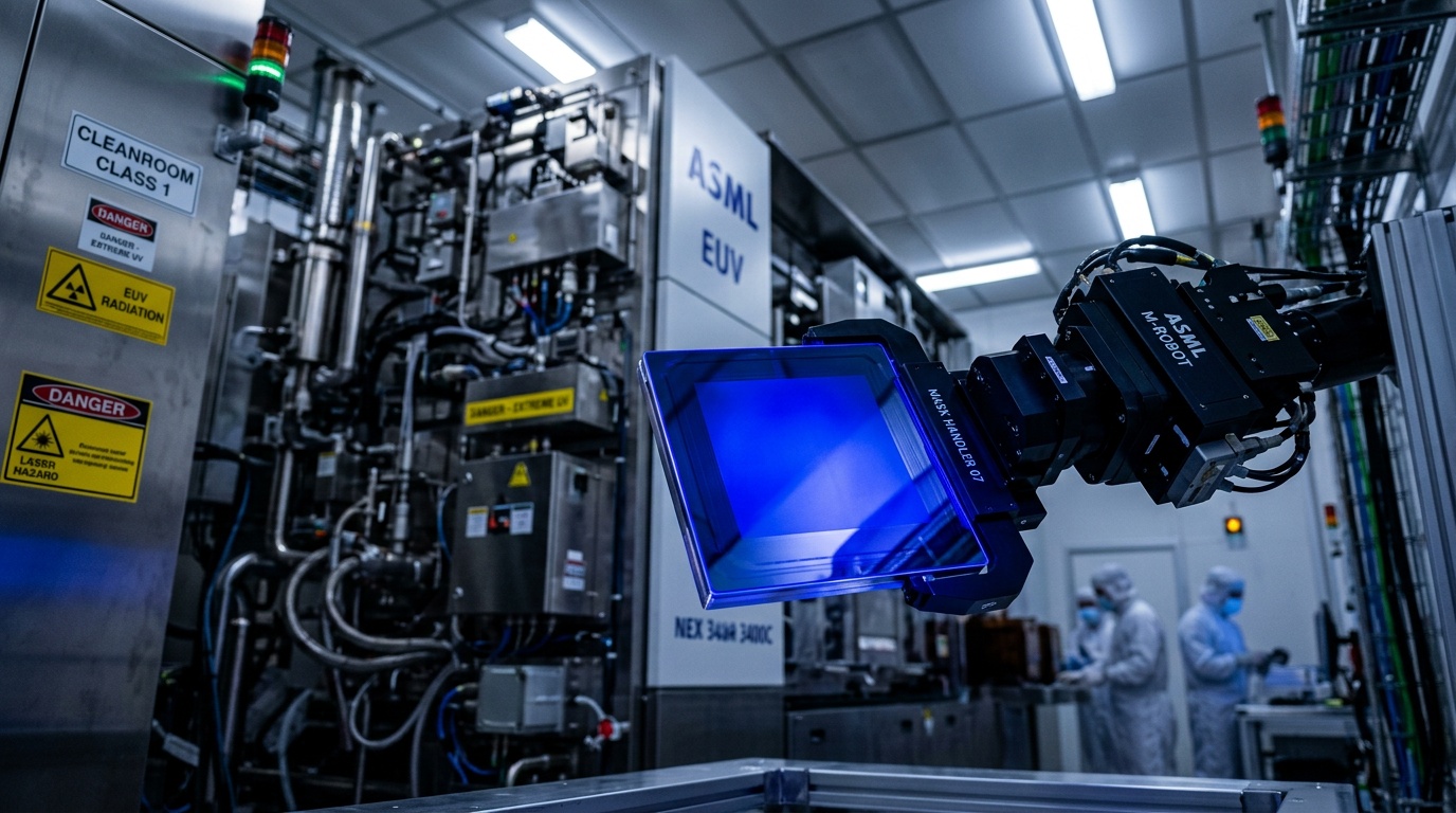
Artificial intelligence is reshaping the semiconductor world, and Samsung Electronics Co. Ltd. (OTC: SSNLF) is making sure it's not left behind. The company is doubling down on advanced chipmaking technology, teaming up more closely with ASML Holding N.V. (NASDAQ: ASML) to push the boundaries of what's possible in memory and logic chips.
The core of this expanded partnership revolves around High Numerical Aperture Extreme Ultraviolet lithography, or High NA EUV for short. It's a next-generation manufacturing technique that promises better resolution and efficiency, which is exactly what's needed as AI demands more powerful and cost-effective chips.
Samsung Joins 12-Inch Photomask Push
One of the big moves here is Samsung joining an industry initiative to develop 12-inch photomasks. That might sound like a small detail, but it's actually a significant shift. The semiconductor industry has been using 6-inch photomasks for decades, and moving to a larger format is a big deal.
Why does size matter? Larger masks, when combined with High NA EUV, can increase factory productivity and lower chipmaking costs. They also eliminate something called "stitching constraints," which is a technical hurdle that limits how chips are patterned. The idea is that this transition will help manufacturers get more out of High NA EUV and make future leading-edge chips more economical to produce.
Samsung isn't doing this alone. It plans to work with ASML and other industry partners to develop the necessary mask technologies and supporting infrastructure. Samsung brings a lot to the table here, with expertise in both memory and foundry manufacturing, plus hands-on experience using advanced EUV lithography.
Samsung Targets High NA DRAM Production By 2028
But the photomask news is just part of the story. Samsung also announced plans to introduce ASML's High NA EUV technology into high-volume DRAM manufacturing by 2028. If it pulls that off, it would be the industry's first such deployment.
The pitch is that High NA EUV's improved resolution will extend the DRAM scaling roadmap, which is a fancy way of saying it'll help keep making memory chips smaller and denser. It also simplifies manufacturing processes and increases efficiency, which is music to any chipmaker's ears.
The two companies are also exploring further collaboration across advanced memory and new manufacturing approaches. It's a broad partnership that goes beyond just one product line.
Samsung Electronics Vice Chairman and CEO Young Hyun Jun summed it up nicely, saying AI is increasing the importance of technological innovation throughout the semiconductor supply chain. ASML CEO Christophe Fouquet echoed that sentiment, calling Samsung one of the company's most important long-term innovation partners and noting that closer cooperation will become increasingly important as AI reshapes semiconductor demand.
Investors seemed to like the news. ASML Holding shares were up 2.95% at $1765.50 during premarket trading on Tuesday.
This is a story about positioning for the future. AI isn't just a buzzword anymore; it's driving real changes in how chips are made. And Samsung is making sure it has the right tools and partners to stay ahead of the curve.